Break through the limits of semiconductor technology? US researchers to achieve 1nm process technology
Intel, TSMC and Samsung's three semiconductor factories will mass-produce a 10nm process this year. They are progressing even faster to launch a 7nm process next year and a 5nm process around 2020. However, with the upgrading of process technology, the semiconductor process is getting closer to the limit, and the manufacturing difficulty is getting bigger and bigger. The process after 5nm has not reached a definite conclusion until now. The transistor materials and processes need to be updated. In this regard, the United States is at the forefront again. Researchers at the Brookhaven National Laboratory have announced that they have achieved 1nm process manufacturing.

According to a report from EETimes, researchers at the Brookhaven National Laboratory under the United States Department of Energy (DOE) announced the creation of a new world record. They successfully manufactured a printing device with a size of only 1 nm and used an electron beam printing process. Non-traditional photolithographic printing technology.

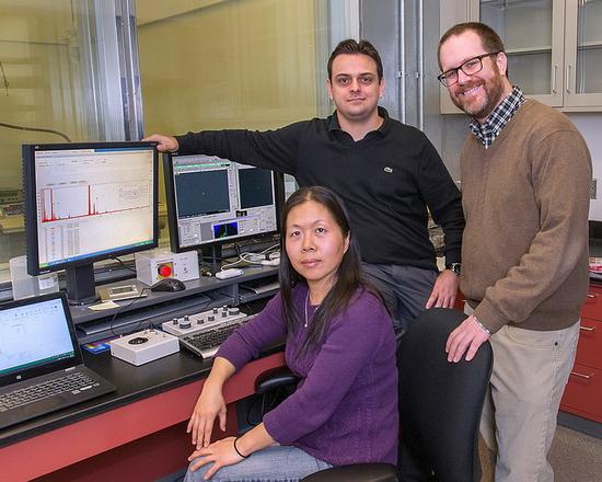
A team that created a 1nm process technology. The woman named Lihua Zhang (a homonym Zhang Lihua, presumably Chinese or Chinese).
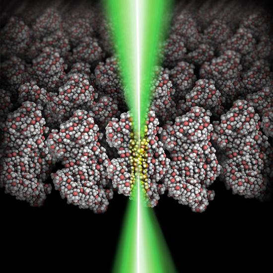
The researchers in this laboratory creatively used electron microscopes to create smaller sizes than the conventional EBL (electron beam printing) process. Electron-sensitive materials are greatly reduced in size by focusing electron beams. The point where you can manipulate individual atoms. The tool they created can greatly change the properties of the material, from electrical conduction to light transmission and interaction in both conditions.
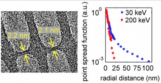
Their achievement was accomplished at the Center for Functional Nanomaterials under the Department of Energy. The 1nm printing uses a STEM (scanned-projection electron microscope), which is separated by 11 nm so that 1 trillion features can be achieved per square millimeter. The density of the features. A 2 nm resolution was achieved with a bias-corrected STEM at a 5 nm half-gate under a hydroxide silicate type resist.
PS: These technologies sound exciting, but the technology developed by the lab does not mean that they can be commercialized quickly. The 1nm process at Bruckheim Lab is different from the current lithography processes, such as the use of electron beams instead of Laser photolithography, the material used is not silicon-based semiconductors but PMMA (polymethyl methacrylate) and the like, the next step they intend to try on silicon-based materials.
In fact, this is not the first time scientists have realized a 1nm process. Last year, Lawrence Berkeley National Laboratory, another national laboratory under the US Department of Energy, announced a 1nm process. They use carbon nanotubes and molybdenum disulfide. And other new materials. Similarly, this technology will not be put into mass production soon, because the carbon nanotube transistors and the PMMA, electron beam lithography here are the same as the current semiconductor process, there are obvious differences, so that manufacturers have to completely eliminate existing equipment This is simply impossible.

Brass Gate Valves Price,1 Inch Brass Gate Valve Price,Brass Gate Valve Price,Brass Gate Valve Price List
AS-SUR INDUSTRIAL VALVE CO., LTD. , https://www.assur-valve.com