Peking University arranges high-density semiconductor carbon nanotubes
The development of integrated circuits requires complementary metal oxide semiconductor (CMOS) transistors to continue to shrink in size while improving performance and reducing power consumption. As mainstream CMOS integrated circuits shrink to the sub-10 nm technology node, it becomes more and more important to adopt new structures or new materials to combat the short channel effect in field effect transistors and further improve device energy utilization efficiency. Among many new semiconductor materials, semiconductor carbon nanotubes have ultra-high electron and hole mobility, atomic-scale thickness and stable structure, and are ideal channel materials for building high-performance CMOS devices. The published theoretical calculations and experimental results show that the carbon tube CMOS transistor can be reduced to a gate length of 5 nm by using a planar structure, and has a 10-fold intrinsic performance-power consumption advantage over silicon-based CMOS devices of the same gate length.
The prerequisite for batch production of carbon nanotube integrated circuits is to achieve ultra-high semiconductor purity (> 99.9999%), tandem, high density (100-200 / μm), and large-area uniform carbon nanotube array film (see Figure 1). For a long time, the limitations of material problems have caused the actual performance of carbon tube transistors and integrated circuits to be far lower than theoretical expectations, and even lag behind silicon-based technology at the same node by at least an order of magnitude, thus becoming the biggest technical challenge facing the field of carbon tube electronics. .
Professor Zhang Zhiyong-Professor Peng Lianmao of the Peking University School of Information Science and Technology / Peking University Carbon-based Electronics Research Center, Key Laboratory of Nanodevice Physics and Chemistry of the Ministry of Education The research group develops new purification and self-assembly methods to prepare high density High-purity semiconductor array carbon nanotube materials, and on this basis, for the first time, the performance of transistors and circuits that surpass the silicon-based CMOS technology of the same gate length has been achieved, demonstrating the advantages of carbon tube electronics. The research group used multiple polymer dispersion and purification techniques to obtain ultra-high-purity carbon tube solutions, and combined with the dimension-limiting self-alignment method to prepare a density of 120 / μm, a semiconductor purity of 99.99995%, and a diameter distribution on a 4-inch substrate 1.45 ± 0.23 nm carbon tube array (see Figure 2), so as to meet the needs of ultra-large-scale carbon tube integrated circuits. Based on this material, field effect transistors and ring oscillator circuits were prepared in batches. The peak transconductance and saturation current of 100nm gate-length carbon tube transistors reached 0.9 mS / μm and 1.3 mA / μm (VDD = 1V, see Figure 3) The sub-threshold swing at room temperature is 90 mV / DEC; a fifth-order ring oscillator circuit is prepared in batches with a yield of more than 50% and a maximum oscillation frequency of 8.06 GHz far exceeding the published nanomaterial-based circuits (see Figure 4) Beyond similar-sized silicon-based CMOS devices and circuits.
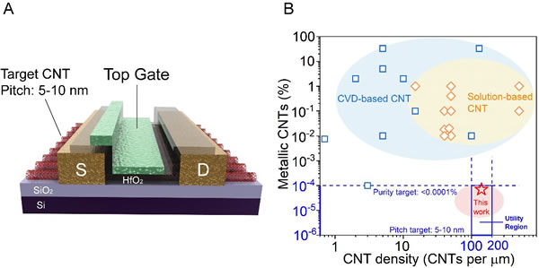
Figure 1. Requirements of large-scale integrated circuits for carbon tube materials
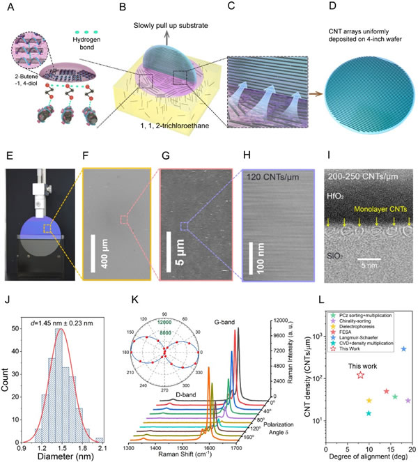
Figure 2. Preparation and characterization of high-density, high-purity semiconductor carbon tube arrays
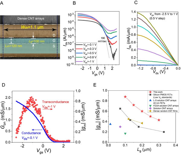
Figure 3. High-performance carbon tube transistor
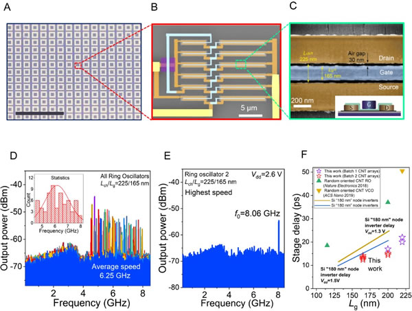
Figure 4. Carbon tube high-speed integrated circuits
This work breaks through the bottleneck that has hindered the development of carbon tube electronics for a long time. The experiments show the performance advantages of carbon tube devices and integrated circuits over traditional technologies for the first time, laying a foundation for the practical development of carbon-based integrated circuits. On May 22, 2020, related research results were titled "Aligned, high-density semiconducting carbon nanotube arrays for high-performance electronics", online Published in "Science" (Science, Volume 368, No. 6493, pages 850 ~ 856); Liu Lijun, a 2015 doctoral student in the Department of Electronics, and Han Jie, an engineer at the Beijing Yuanxin Carbon-based Integrated Circuit Research Institute, are joint first authors, Zhang Zhiyong and Peng Lianmao is a co-corresponding author.
The above research was funded by the National Key R & D Program "Nano Science and Technology" special project, Beijing Science and Technology Program, National Natural Science Foundation of China, etc. Researchers from the Hunan Provincial Advanced Sensing and Information Technology Innovation Institute of Xiangtan University, Zhejiang University, Peking University Nano Optics Frontier Science Center and other units participated in the cooperation.
Wire Stainless Steel Product.
China Kitchen Rack,Sink Grid,Stainless Mesh Storage Baskets,Kitchen Wire Storage, we offered that you can trust. Welcome to do business with us.
Kitchen Rack is made of high quality 304 stainless steel, This kind of material steel luxury, never rust, resist corruption, easily clean, safe, healthy and durable. Prevent rust or chemicals from contaminating food and damaging health
Kitchenware,Bread basket,dish rack,cutting board rack,Sink Grid,dish drying rack
Shenzhen Lanejoy Technology Co.,LTD , https://www.ccls-vaccine.com