Shanghai Institute of Technology, etc. made progress in the study of low-dimensional materials controlled by iron polarization
Modern microchips and sensor devices are important carriers to support today's information society. With advances in technology and processes, higher requirements have been placed on material properties and device structures. In recent years, new low-dimensional materials have appeared, and their unique structures and exotic properties have attracted much attention. They have shown their potential value in the fields of electronics and optoelectronic devices. The physical basis of constructing semiconductor functional devices is to adjust the type and concentration of semiconductor material carriers through element doping. Specific to new low-dimensional semiconductor materials, how to achieve precise control of their carriers is also the only way to achieve their rich functional devices.
Recently, researchers from the Shanghai Institute of Technical Physics of the Chinese Academy of Sciences have collaborated with relevant teams from Fudan University, Nanjing University, East China Normal University and the Institute of Microelectronics of the Chinese Academy of Sciences to propose the use of non-volatile ferroelectric fields for low-dimensional semiconductor materials. New method of precise doping, and using this method to build a variety of new functional electronic and optoelectronic devices.
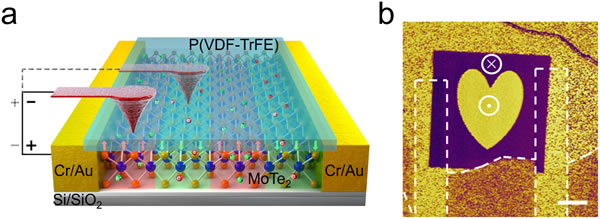
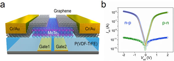
Specifically, the researchers proposed two methods for constructing low-dimensional semiconductor optoelectronic devices using ferroelectric polarization control. First, the ferroelectric thin film is polarized by nanoprobe technology, and then the low-dimensional semiconductor covered by it is controlled (top-down method, see Figure 1). When a positive voltage is applied, the polarization is downward, and electrons are injected into the semiconductor material; when a negative voltage is applied, the polarization is upward, and holes are injected into the semiconductor material. Its characteristics are that the device pattern can be edited arbitrarily, erasable and rewritten, and the spatial size of the doped area is accurate. Based on this method, the researchers built devices such as pn junctions, BJT transistors, and new storage. Second, build a split-gate structure, polarize the ferroelectric thin film through the application of voltage through the solid electrodes, and then regulate the top-layer low-dimensional semiconductor (from bottom to top, see Figure 2). It is characterized by a solid state structure, full polarization, and better device performance and stability. Using the above two technical approaches, both junction photodetectors and photovoltaic devices can be realized, and the detection wavelength of the device can cover the visible-shortwave infrared band.
The method of controlling the carrier of low-dimensional semiconductor by the ferroelectric polarization field proposed in the above work provides a new technical approach for the functional application of low-dimensional semiconductor. Related research results have been published in journals such as Nature-Electronics (doi.org/10.1038/s41928-019-0350-y) and Advanced Materials (doi.org/10.1002/adma.201907937).

Figure 1. Nanoprobe manipulates a low-dimensional semiconductor homojunction controlled by ferroelectric domains (implemented from top to bottom)

Figure 2. Split-gate controlled low-dimensional semiconductor pn junction solid-state structure (from bottom to top)
Led Pixel Light,Smart Pixel Light,Full Color Rgb Led Pixel Light,Waterproof Smart Pixel Light
Shen zhen SH LED Technology Co.,Ltd , https://www.pixellightsolutions.com