New laser diamond tool for machining ceramic and semiconductor materials
Dr. John Patten, professor of manufacturing engineering at Western Michigan University, developed a microlaser-assisted processing technique called "μ-LAM" that combines laser and diamond tools to heat and soften silicon semiconductors and ceramic materials. Cutting processing.
According to John Patten, “These materials are usually very brittle. If they are tried to deform or process them, they tend to break easily. By softening these materials, we can increase their flexibility and make them easier to process. â€
The μ-LAM processing unit integrates an infrared fiber laser (wavelength range 1000-1500 nm). The laser beam is irradiated onto the workpiece through a single point diamond tool with high optical clarity to heat the workpiece material above 600 °C. Diamond tools with a radius of 5 μm to 5 mm are bonded by epoxy (for milliwatt laser power processing) or by soldering/brazing (for processing of 1 watt or more laser power). Connect to a laser mounted in a tungsten or carbide housing.
Other engineers and technicians have tried to process brittle materials (such as ceramics) in a variety of different ways. One method is to first heat the workpiece in the furnace and then process it; the other method is to use laser heating and diamond tool cutting, respectively. The method invented by Patten combines laser and diamond tools, which has significant advantages. He explained, “Things are much simpler, because the laser is aligned with the tool itself, and the laser is heated just at the cutting edge of the tool, so that the best results can be obtained. In addition, the workpiece material is not excessive. heating."
According to Patten, μ-LAM processing technology can also cut processing time and processing costs and achieve a very smooth optical surface. “When using conventional machining methods, if you want to make an optical component (such as a mirror), you usually need to start with casting the workpiece blank and then carry out a series of processing steps: rough grinding, fine grinding, grinding, and finally forming. The machining method replaces the original series of processes, cutting with a single-point diamond tool on CNC machine tools, and also achieves excellent surface roughness (Ra1-10nm)."
Patten is working with a Japanese company to commercialize the μ-LAM system. He expects the invention to find its place in a number of industries, including automotive, aerospace, medical equipment, semiconductors and optics. “Our initial goal was to target the optical and semiconductor industries, but now it seems that most of its applications will be on high-energy, high-temperature microelectronics. In the semiconductor industry, silicon is the carrier of chips and integrated circuits,†he said. At higher temperatures, silicon carbide is used. Therefore, almost all of our energy is now focused on the processing of silicon carbide.
We are manufacturing high transmission and durability domes. BK7 or HK9L Glass domes are often used in meteorology applications. Fused silica domes are commonly used in underwater applications at extreme environments. Other application for our dome include meteorology applications, pyranometers, defence applications and as high pressure view ports in underwater cameras and submersibles.

Material:Optical glass N-BK7 , H-K9L, UV Fused Silica, Sapphire, and infrared crystal materials.
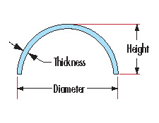
Diameter:20-350mm
Diameter Tolerance:+/-0.1mm
Thickness:>2mm
Thickness Tolerance±0.2~0.1mm
Center Deviation:3-5'
Surface quality:80/50 60/40
Coating: Antireflection Coating inside
Chamfers:0.2 x 45° typical
Hemisphere Dome Lens,Hemispheric Glass Domes Lens,Optical Glass Hemisphere Domes Lens,120 Mm Diameter Glass Dome Lens
China Star Optics Technology Co.,Ltd. , https://www.csoptlens.com