D/A conversion technology scheme using PDM
1 Introduction
In digital signal processing, it is often necessary to convert a multi-bit digital signal into a one-bit digital signal. For example, in the field of communications, the receiver receives the encoded digital speech signal and converts it to an analog signal, ie, the original analog speech signal is restored. The encoded speech signal is usually a multi-bit bit stream. Therefore, how to convert a multi-bit bit stream into an analog voice signal becomes the key to ensuring communication quality. As another example, in some control circuits, the control signals are multi-bit digital signals that are calculated and generated, and these digital signals must be converted into analog signals to control the circuit. Therefore, how to convert multi-bit digital signals into analog signals that meet the actual requirements becomes the most concerned issue for control circuit designers.
In the traditional circuit design, in the face of the above problems, it is usually chosen to use a D/A converter composed of a plurality of separate electronic components, and sometimes we call it a static D/A converter. However, due to the composition of the static D/A converter, it is determined that he must occupy a certain amount of space and consume a certain amount of power in the system. Therefore, in those system schemes that require portability, the static D/A converter has to be replaced [1].
So people choose the so-called "digital basis" D / A converter. There are two methods for digital D/A conversion: PWM (Pulse Width Modulation) pulse width modulation and PDM (Pulse Density Modulation) pulse density modulation. This digital D/A converter occupies less physical space and consumes less power. Therefore, it is suitable for systems with strict system hardware size and power consumption requirements [1].
As early as the 1940s, PWM began to be used in the phone. Due to the limitations of PWM, people have proposed a PDM modulation method twenty years later. However, since the application market at that time was still not large, this modulation method has not been widely concerned and applied. In recent years, digital technology has been widely used in various fields, digital products are developing rapidly, and digital signal processing has begun to receive more and more attention. Therefore, PDM modulation technology has been re-emphasized and applied in different fields.
2 PDM basic introduction
PDM is a modulation method that provides analog signals in the digital domain. In the PDM signal, a logic "1" indicates a single pulse, and a logic "0" indicates no pulse. Usually logic "1" and logic "0" are discontinuous, and logic "1" is more evenly distributed in each modulation signal period. The single pulse does not represent the amplitude, and the density of a series of pulses corresponds to the amplitude in the analog signal. A PDM signal consisting entirely of "1" corresponds to a positive amplitude voltage; a PDM signal consisting entirely of "0" corresponds to a voltage of negative amplitude; a signal consisting of alternating "1" and "0" is Corresponds to a voltage of 0 amplitude.
3 PDM implementation

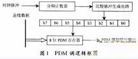
The logic block diagram of PDM modulation technology is shown in Figure 1. A frequency division counter is used to realize a clock signal that meets the requirements of the actual application, and the pulse period is ΔT. Then, the clock signal is sent to the N-bit counter to realize the counting of 0, 1, ..., 2N-1. In the single pulse period ΔT of the counting, the logic value at each bit of the counting result is subjected to a series of logic operations to realize the N-bit comparison reference pulse signals, which are Bit0, Bit1, Bit2, ..., Bit(N -1), respectively. It is worth noting that in each ΔT, there is only one bit with a logic "1" and the other bits with a logic "0". At the same time, the N-bit bus data outputted from the register is compared with the comparison reference pulse signals Bit0, Bit1, Bit2, ..., Bit(N-1) bit by bit, and the result on each bit is ORed to obtain the modulation in ΔT. result. Thus, the modulation result is obtained after the end of the entire modulation period.
For a digital signal of N bits, the modulation period T = 2N · ΔT. For an 8-bit digital pending signal, the modulation result for each pulse period ΔT is:

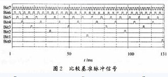
For example, an 8-bit hexadecimal digital signal "1AH" is modulated. The comparison reference pulse signal as shown in Fig. 2 is generated by an 8-bit counter. Obviously, in each pulse period ΔT, only one bit in Bit0~Bit7 has a pulse.

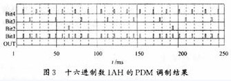
The binary number corresponding to the hexadecimal number "1AH" is "00011010", Bit4, it3, and Bit1 are "1", and all other bits are "0". After bitwise logical operation, that is:

After a modulation period modulation, a modulated signal as shown in FIG. 3 is obtained. Such an 8-bit digital signal is converted into a 1-bit pulse signal.

NINGBO DURREX PUMPS CO.,LTD , https://www.durrexlobepump.com